Email Us
+86-755-23021813
david@hx-technology.com
English

Blog

  • Apr,15,2022

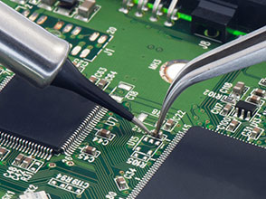
    Best Welding Method for Printed Circuit Board
    Ⅰ. The effect of tinning on printed circuit boardsWhen the hot liquid solder dissolves and penetrates into the metal surface to be welded, it is called metal tinning or metal tinning.The molecules of...
  • Apr,08,2022

    What is PCB?
    Printed circuit board (PCB) will appear in almost every electronic device. If there are electronic parts in a specific device, they are all mounted on PCBs of different sizes. In addition to fixing va...
  • Mar,22,2022

    Manufacturing Process of Bms PCB
    Bms PCBs integrate traditional technologies and techniques such as mechanical, electrical, automation, chemical, biological, ERP, cost, management, and environmental protection as a distinctive proces...
  • Mar,08,2022

    Solutions to PCB Short Circuit
    PCB "line short circuit" is an issue that PCB manufacturers will face practically every day, but it is also a more difficult problem to address, the problem of improving good or poor, direct...
  • Feb,22,2022

    PCB Circuit Board Design Guidelines
    The bms PCB is the support and electrical connection of circuit components and equipments in electronic products. With the rapid development of electronic technology, the density of bms PCB is getting...
  • Feb,08,2022

    PCB Design Requirements
    Ⅰ. The process of PBC design The pbc design is the process to convert a circuit schematic into a diagram of bms PCB and determine processing technical requirements according to the intent of designer...
  • Jan,18,2022

    High Precision Multi-layer Theremin PCB Processing
    With the development of modern electronic technology and the high-speed and integration of chips, the inside and outside electromagnetic environment of various electronic equipment systems has become ...
  • Jan,04,2022

    The Cause of Theremin PCB Circuit's Bent
    When the theremin PCB is designed, many of the layout lines are bent. What is the reason for the THEREMIN PCB circuit design to be bent? There are three main reasons.1. Reduce the area of the theremin...
  • Dec,21,2021

    The Wiring, Welding Skills and Notices of the Theremin PCB
    Ⅰ. Wiring and soldering skills of theremin PCB1. The edges of the input end and output end of the theremin PCB should be perpendicular to each otherThe edges of the input end and the output end shoul...
Contact Us
Phone: +86-755-23021813
Address: 6th floor, Huachuangda YiJing Building, 45 District, Bao'an District, Shenzhen, China, 518101
6th floor, Huachuangda YiJing Building, 45 District, Bao'an District, Shenzhen, China, 518101
david@hx-technology.com
+86-755-23021813