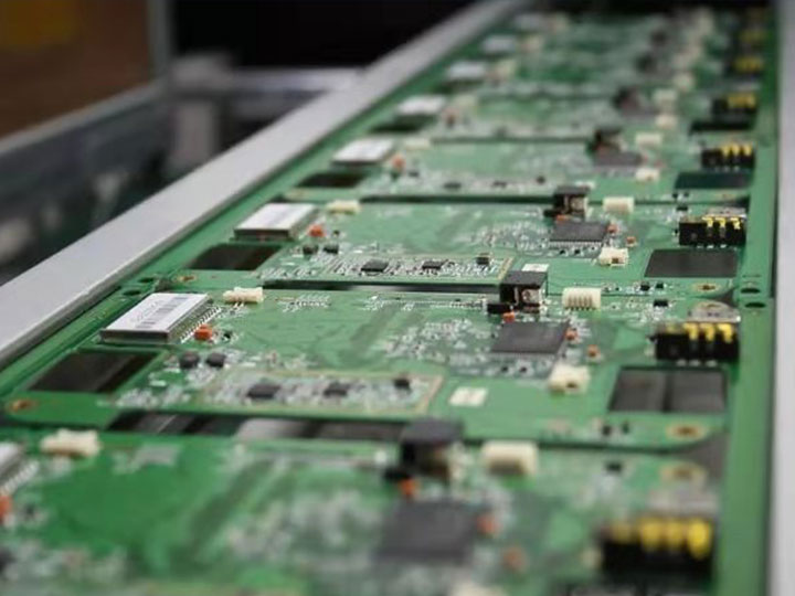
Printed circuit board (PCB) serves as the foundation for most electronic products, with a simple structure that's most commonly associated with computer hardware. However, it is also used in radios, televisions, cellphones, and more. A PCB's performance depends on factors such as manufacturing materials, cost, prototype, and more.
Additionally, PCB thickness plays a critical role in overall performance and durability, affecting the board's resistance and conductivity. Working with perfect thickness is therefore essential, as whenever we talk about "standard" features or benchmark measurements for certain projects, it's what we hope to achieve with ideal characteristics. Our product must pass all performance, weight, durability, reliability, and most importantly, quality tests.
The current standard PCB thickness falls within the following range: 0.031 inches (0.78 millimeters), 0.062 inches (1.57 millimeters), and 0.093 inches (2.36 millimeters). However, the most commonly used thickness is 0.063 inches (1.57 millimeters). It's important to note, however, that board thickness standards are also determined by the users or applications. Initially, laminates were used as substrates, resulting in greater thickness. With technological advancements, better options such as epoxy resin emerged.
The most important and widespread metal used in PCB function and application is copper. This is because using copper creates a relatively smoother standard board thickness, at approximately one ounce. Furthermore, ultra-thin security PCB thickness can limit available surface-treatment options. There are various manufacturing and design specifications and factors to be mindful of, with some being design factors that impact PCB thickness.
Significant cost factors: determined by factors such as board size and layer count;
PCB complexity: layer count, through-hole count;
Material used: material choice based on operating speed, frequency, operating temperature (maximum);
Operational environment: manufacturing factors, hole size and count, copper thickness, surface treatment that impact PCB thickness.
A trace width calculator is used to specify the PCB thickness. It functions similar to a regular calculator, requiring input of details and specifications, where it provides the desired thickness for you. In order to make accurate and effective determinations, the calculator offers up to decimals (one hundredth of a millimeter) in calculation ability. However, if the application specifies that the thickness must remain under a measurement value, the calculator will adjust accordingly.
Here are some factors and specifications to keep in mind when deciding on the thickness of a PCB board for better durability and performance: weight, flexibility, impedance match, required components space, compatibility. Factors to keep in mind when customizing security PCB thickness:
Turnaround time: typically, there are more expected turnaround times for customized PCB layer thickness, due to the unusual thickness specifications. This will affect your delivery schedule and development time.
Equipment capability: Be cautious when choosing your equipment if you don't want to compromise on your design and models. If you use limited equipment to manufacture and design the typical PCB thickness you are looking for, you'll have to compromise and modify your PCB layout.
Additional costs: Extra costs are typically incurred due to extra details and expectations. Using specific materials, designs, and adhering to a detailed set of instructions equates to generating an additional manufacturing cost compared to the regular price.
Using customized thickness can increase design appeal and yield, providing it with unique performance and value. However, using multilayers can be incredibly costly due to additional handling, manufacturing steps, and materials. Having the perfect manufacturing partner in place can smoothly achieve the desired thickness. The first step in customization usually involves identifying common core prepreg thickness and perfectly combining them with plated copper, copper foil, and solder-resist layers.