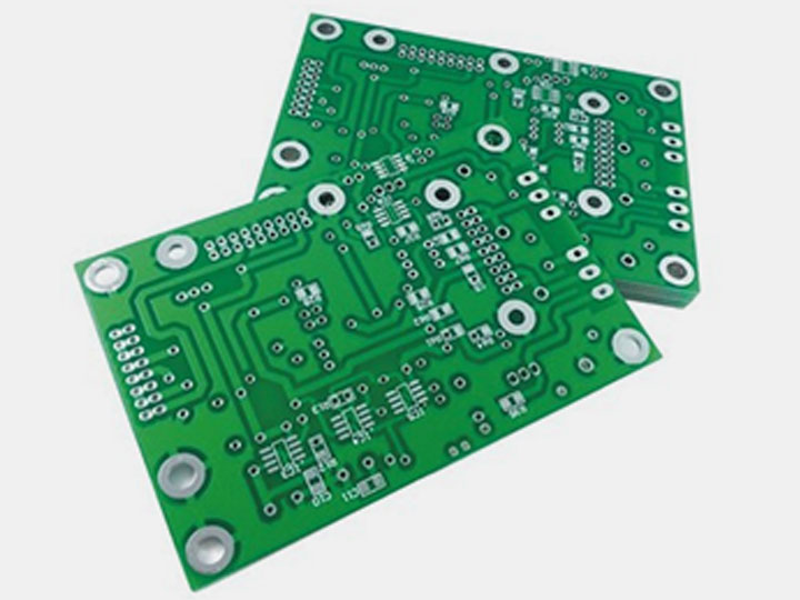
PCB telecom is the provider of electrical connection of electronic components. It has the characteristics of high wiring density, lightweight, thin thickness, and good bending. And it can make the circuit miniaturized and intuitive, which plays a vital role in the mass production of fixed courses and optimizing the layout of electrical appliances. Various matters need to be paid attention to in circuit board welding. Otherwise, it is easy to cause damage to the PCB board or components. What about the welding process of PCB telecom?
1. Welding materials
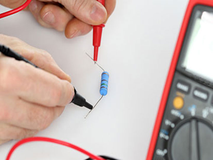
(1) Solder: sn60 or Sn63 solder is conforming to general standards, or hl-snpb39 tin-lead solder is usually used.
(2) Flux: rosin flux or water-soluble flux can usually be used, and the latter is generally only used for wave soldering.
(3) Cleaning agent: it shall ensure no corrosion and pollution to the PCB telecom. Generally, absolute ethanol, trichlorotrifluoroethane, isopropanol, aviation washing gasoline, and deionized water shall be used for cleaning. The specific cleaning agent shall be selected according to the process requirements.
2. PCB telecom welding tools and equipment
(1) The reasonable selection of power and type of electric soldering iron is directly related to improving welding quality and efficiency of BMS PCB board.
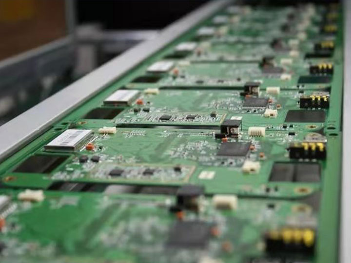
(2) Wave soldering machines and reflow soldering machines are welding equipment suitable for industrial mass production.
3. Preparation before welding
(1) Check whether the model, specification, and quantity of components meet the requirements according to the list of components.
(2) The welding personnel shall wear anti-static wrist and confirm that the constant temperature soldering iron is grounded.
4. Assembly and welding sequence
The assembly and welding sequence of components of PCB telecommunication: a resistor, capacitor, diode, triode, integrated circuit, and high-power transistor, and other details are small first and then prominent.
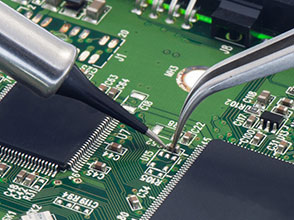
Manual plug-in, manual welding, repair, and inspection are mainly required in the welding process of BMS PCB.
(1) Select the corresponding model according to the production task and check whether the model of the incoming PCB telecom is correct and whether the circuit board is damaged.
(2) Check whether the surface of the PCB telecom is clean and free of dust, oil stain, fingerprint, etc. If it is not clean, it can be properly cleaned with alcohol.
(3) Select corresponding devices and carefully check the model and quantity of machines. At the same time, check whether there are damage or rust marks on the device surface and pins and other factors affecting the device performance.
(4) After the model and quantity of the device and PCB telecom are confirmed, plug the device into the circuit board according to the correspondence between the device label and the position on the circuit board.
(5) Weld all devices according to the welding requirements to ensure no missing welding, false welding, etc.
(6) Cut off the excess pins after welding the PCB telecom.
(7) Check all welding joints for nonconformities and repair them, if any.
(8) After welding, the PCB telecom must be thoroughly cleaned in time to remove residual flux, oil stain, dust, and other dirt. The specific cleaning shall be carried out according to the process requirements.