

The bms PCB is the support and electrical connection of circuit components and equipments in electronic products. With the rapid development of electronic technology, the density of bms PCB is getting higher and higher. The quality of bms PCB planning has a great impact on the effectiveness of anti-disturbance. Therefore, when planning the bms PCB, it is necessary to follow general principles of bms PCB planning and meet requirements of anti-disturbance planning.
The layout of components and wires is very important for optimal performance of electronic circuits. In order to design the bms PCB with high quality and low cost, we should follow these general principles.
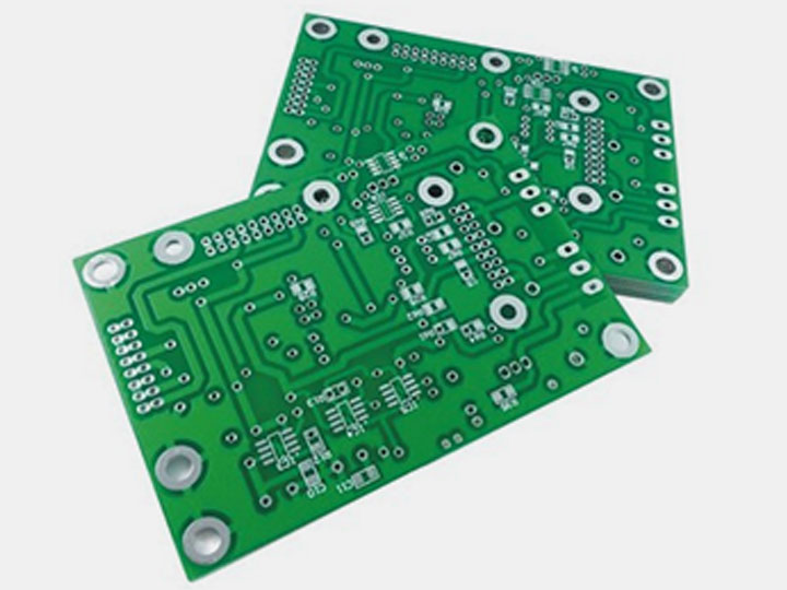
Layout: Firstly, consider the size of bms PCB. If the size is too large, the printed wirings will be long, the impedance will increase and the noise immunity will decrease, so the cost will increase. If the size is too small, the heat dissipation is poor and the adjacent wirings are susceptible to interference. After determining the size, it is necessary to determine the location of special components. Finally, according to the functional units of circuit, all the components of circuit are laid out.
1. Shorten connections among high-frequency components as much as possible and try to reduce their distribution parameters and electromagnetic interference with each other. Easily disturbed components should not be too close to each other, and input and output components should be as far away as possible.
2. Some components or wires may have a high potential difference, whose distance should be increased to avoid the accidental short-circuit resulted from the discharge of bms PCB. Components with high voltage should be placed in sites not easily accessible by hand during debugging.
3. Components weighing more than 15g should be secured with a support and then welded. Those large and heavy, calorific components should not be installed on the bms PCB and ought to be fixed on the chassis of case and consider the heat dissipation. Thermal elements should be kept away from heating elements.
4. The layout of adjustable components such as potentiometers, adjustable inductor coils, variable capacitors and micro switches should consider the structural requirements of the whole machine.
If it is adjusted in the machine, it should be placed above the bms PCB for easy adjustment. If it is adjusted outside the machine, its position should be adapted to the position of the adjusting button on the panel.
5. The position occupied by locating hole and fixed bracket of bms PCB board should be reserved.
1. Arrange the position of each functional circuit unit according to the circuit process, so that the layout is convenient for signal flow and keeping the signal as consistent as possible.
2. PCB assembly factory takes the core components of each functional circuit as the center, around it to carry out the layout. Components should be evenly, neatly and compactly arranged on the bms PCB. Minimize and shorten leads and connections among components.
3. For circuits operating at high frequencies, the distribution parameters among components should be considered. In general circuits, components should be arranged in parallel as much as possible. In this way, not only beautiful, but also easy to load and unload, easy to mass production.
4. A component located on the edge of a circuit board, usually not less than 2mm from the edge of a circuit board. The best shape for a bms PCB is a rectangle.
The ratio of length to width is 3:2 and 4:3. When the size of the circuit board surface is greater than 200x150mm, the mechanical strength of the circuit board should be considered.