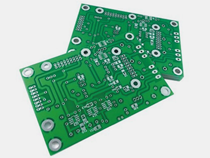

In PCB circuit design, special components refer to key components in the high-frequency part, core components in the circuit, components susceptible to interference, components with high voltage, components with high heat generation, and some special-shaped components. Components, the location of these special components need to be carefully analyzed, so that the layout meets the requirements of circuit functions and production needs. Improper placement of them may cause circuit compatibility issues, signal integrity issues, and lead to PCB design failure.
When designing how to place special components, first consider the size of the PCB. When the PCB size is too large, the printed lines will be long, the impedance will increase, the anti-noise ability will decrease, and the cost will also increase; if it is too small, the heat dissipation will not be good, and the adjacent lines will be easily disturbed. After determining the size of the PCB, determine the placement of special components. Finally, according to the functional unit, all the components of the circuit are laid out. The location of special components on printed circuit boards generally follows the following principles when laying out:
1. Shorten the connection between high-frequency components as much as possible, and try to reduce their distribution parameters and mutual electromagnetic interference. Components that are susceptible to interference cannot be too close to each other, and the input and output should be as far away as possible.
2. Some components or wires may have a high potential difference, and the distance between them should be increased to avoid accidental short circuit caused by discharge. High-voltage components should be kept out of reach of hands as much as possible.
3. Printed circuit board components weighing more than 15G can be fixed with brackets and then soldered. Those heavy and hot components should not be placed on the circuit board, but should be placed on the bottom plate of the main chassis, and the heat dissipation problem should be considered. Heat-sensitive components should be kept away from heating components.
4. For the layout of adjustable components such as potentiometers, adjustable inductance coils, variable capacitors, and micro switches, the structural requirements of the entire board should be considered. Some frequently used switches should be placed if the structure permits. within easy reach. The layout of components should be balanced, dense and not top-heavy. The success of a product, one must pay attention to the internal quality. The second is to take into account the overall aesthetics. Only when both are relatively perfect can a board become a successful product.
1. Placed on components that are closely matched to the structure, such as power sockets, indicator lights, switches, connectors, etc.
2. Place special components, such as large components, heavy components, heating components, transformers, ICs, etc.
3. Place small components.
1. Whether the size of the printed circuit board is consistent with the processing size required by the drawing.
2. Whether the layout of the components is balanced, neatly arranged, and whether they have all been laid out.
3. Whether there is any conflict at all levels. Such as whether the components, outer frame, and layers that require silk screen printing are reasonable.
4. Whether the commonly used components are convenient to use. Such as switches, plug-in board insertion equipment, components that need to be replaced frequently, etc.
5. Is the distance between heat sensitive components and heating components reasonable?
6. Whether the heat dissipation is good.
7. Whether the line interference problem needs to be considered.