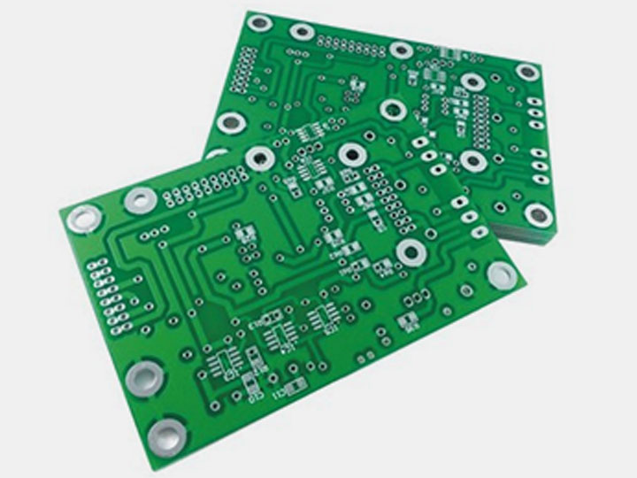
For PC motherboards and display cards, the most basic part is the printed circuit board (PCB: Printed Circuit Board), which is the basis for the work of various boards. For specific products, the design and manufacturing level of the printed circuit board greatly determines the indicators and final performance of the product. This article will introduce the basic knowledge of PCB, including the relevant terminology and classifications. I hope it will help friends to understand.
Printed Circuit Board (PCB: Printed Circuit Board) is the basis of almost any electronic product and is found in almost every kind of electronic device.
Generally speaking, if there are electronic components in a certain kind of equipment, then they are also mounted on PCBs of various sizes.
In addition to fixing various components, the main role of the PCB is to provide the connection circuit between the components. As electronic devices become more and more complex and require more and more components, the lines and components on the PCB are becoming denser.
The circuit board itself is made of insulated and unbendable material, and the fine wiring material that can be seen on the surface is copper foil. Before being processed, the copper foil is covered with the entire board, and during the process by PCB fabrication companies. The middle part is etched off, leaving the part that is left behind to become a network of tiny lines. The printed circuit board is named after the process of forming the outline for etching, which is mostly done by printing. These lines are called conductor patterns and are used to provide circuit connections for the components on the PCB.
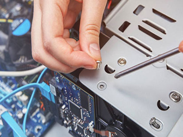
In order to fix components to the PCB, their pins need to be soldered directly to the wiring. On the most basic PCB (single-sided), the components are concentrated on one side and the wires are concentrated on the other side. In this way, it is necessary to punch holes in the board so that the pins can pass through the board to the other side, so the component pins are soldered on the other side. Because of this, the front and back of the PCB is called the component side (Component Side) and solder side (Solder Side).
For some of the components that may need to be frequently unplugged, such as the CPU on the motherboard, the need to give users the option to adjust, upgrade, you can not directly weld the CPU on the motherboard, then you need to use the socket. Although the socket is directly welded to the board, the components can be removed and installed at will. The socket, as shown below, allows components (here referring to the CPU) to be easily inserted into the socket and removed. The fixing bar next to the socket can hold the component in place after you insert it.
PCB connection
If two PCBs are to be connected to each other, i.e., two PCBs are physically connected in a circuit, the edge connector, commonly known as the "gold finger",
is generally required. Gold fingers contain a number of exposed copper pads, -- these copper pads are in fact part of the PCB wiring. The gold finger on one PCB is inserted into a suitable slot on the other PCB (generally called the expansion slot Slot). In the computer, such as display cards, sound cards, or other similar interface cards, are connected to the motherboard through the gold finger.
For theremin PCB, there are various ways to classify them, among which the classification according to the number of layers is the most common.
Single-Sided Boards
As we mentioned earlier, in the most basic PCB, the components are concentrated on one side and the wires are concentrated on the other side. Because the wires only appear on one side, so we call this PCB called single-sided (Single-sided). Relatively speaking, single-sided in the design of many limitations (because there is only one side, between the wiring can not cross and must be wrapped around a separate path), in dealing with complex circuits are often unable to cope, and is now rarely used, unless the circuit is really very simple.
Double-Sided Boards
This board has wiring on both sides. However, to use the wires on both sides, there must be a proper circuit connection between the two sides to work. This circuit between the "bridge" is called the guide hole (via). Conductor holes are small holes in the PCB, filled or coated with metal, which can be connected to the wires on both sides. Because the double-sided board is twice as large as the single-sided board, and because the wiring can be interleaved (can be wrapped around to the other side), it is more suitable for use in more complex circuits than the single-sided board.
Multi-Layer Boards
In order to increase the area that can be wired, multi-layer boards use more single or double-sided wiring boards. Multi-layer boards use several double-sided boards with a layer of insulation placed between each layer and then glued (laminated). The number of layers on the board represents how many separate layers of cabling are present, usually an even number of layers and containing the outermost two layers. Most mainframe boards are 4 to 8-layer structures, although it is technically possible to achieve nearly 100-layer PCBs. Large supercomputers mostly use quite a multi-layer motherboard, but because such computers can already be replaced by many groups of ordinary computers, ultra-layer boards have gradually fallen out of use. For multilayer boards, because the layers in the PCB are tightly integrated, it is generally less easy to see the actual number.