PCBA technology has penetrated into almost every terminal field of the electronics industry, including computers, communications, consumer electronics, industrial control, medical instruments, national defense, aerospace and many other fields. PCBs have developed from single layer to double-sided, multi-layer and flexible, and still maintain their respective development trends. Due to the continuous development in the direction of high precision, high density and high reliability, continuous reduction in size, cost reduction and performance improvement, printed boards still maintain a strong vitality in the future development of electronic equipment.
1. Preliminary preparation: including preparing the component library and schematic diagram. Before designing the PCB, first prepare the schematic SCH component library and the PCB component package library.
2. PCB structure design: According to the determined circuit board size and various mechanical positioning, draw the custom pcb enclosure in the PCB design environment, and place the required connectors, buttons/switches, screw holes, assembly holes, etc. according to the positioning requirements.
3. PCB layout design: The layout design is to place the devices in the PCB frame according to the design requirements. Generate a netlist in the schematic tool, and then import the netlist in the PCB software. After the netlist is successfully imported, it will exist in the software background. All devices can be called out through operations, and there are flying wires between each pin to prompt connection. At this time, the layout design of the device can be carried out.
4. PCB wiring design: PCB wiring design is the process with the largest workload in the entire custom PCB design, which directly affects the performance of the PCB board.
5. Wiring optimization and silk screen placement: The general design experience is that the time for optimizing wiring is twice the time for initial wiring. After the PCB wiring optimization is completed, post-processing is required. The first thing to deal with is the silk screen logo of the PCB layout. When designing, the bottom silk screen characters need to be mirrored to avoid confusion with the top silk screen.
6. Network DRC inspection and structural inspection: Quality control is an important part of the PCB circuit board design process. General quality control methods include: design self-inspection, design mutual inspection, expert review meetings, special inspections, etc.
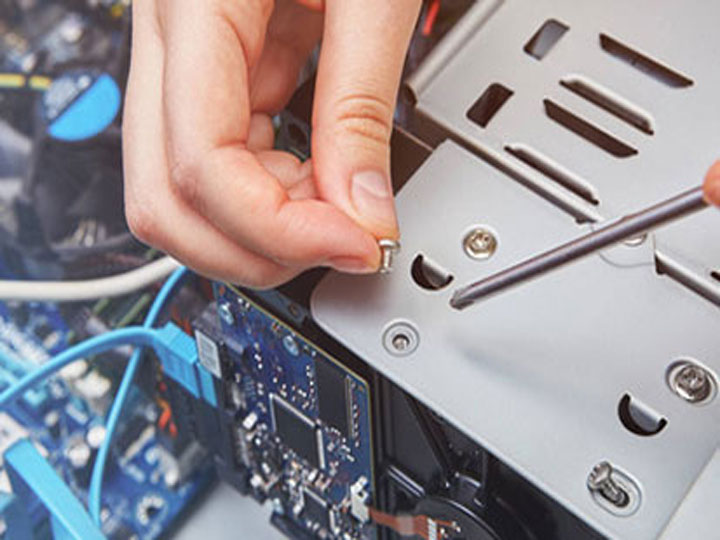
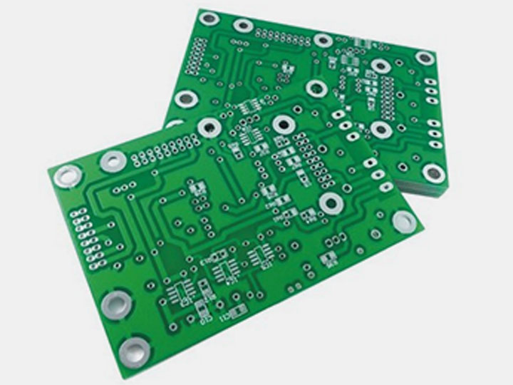
7. PCB board making: Before the PCB board is officially processed, the circuit board designer needs to communicate with the PE of the PCBA company to answer the manufacturer's confirmation questions about the PCB board processing. These include but are not limited to: selection of PCB sheet types, adjustment of line width and spacing of circuit layers, adjustment of impedance control, adjustment of PCB stack thickness, surface treatment process, aperture tolerance control and delivery standards, etc.