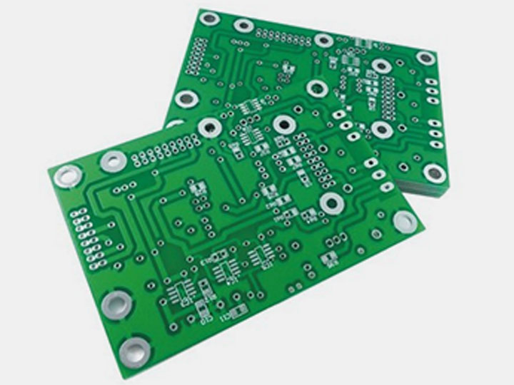
Single-sided, double-sided, and multilayer are the three main types of PCB (printed circuit board). A PCB assembly involves several individual stages, all of which need to work together as a team to produce an overall integration process. Each stage needs to enter the next stage, and feedback after the final stage is necessary to maintain the quality. This way, any problems can be quickly identified, and necessary adjustments made. This is an overview of the PCB assembly process.
Before adding any components to the board, solder paste must be added to the necessary areas. Some of these areas include component pads, where solder is added using a solder stencil. The solder paste comes in the form of tiny solder particles with a flux. This mixture is added to the appropriate locations in a similar way to a typical printing process. By moving the flow channels on the screen, the solder paste will seep through the screen holes and deposit onto the PCB board. Note that solder deposits are only found in the solder pads. This is because the PCB files are used to generate the solder stencils. Thus, the solder stencil holes always align with the pads. To achieve the best results in PCB manufacturing, it is necessary to monitor the solder amount to ensure the correct volume enters the resulting joints.
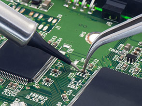
In this part of the PCB manufacturing and assembly process, the circuit board will undergo a process called pick and place. A pick and place machine picks up the components from the distributor and places them in the required positions on the board. The tension in the solder paste helps to keep all the components in the correct position without the PCB moving. To secure the components to the board, some pick and place machines will add glue drops during the PCB manufacturing process. To avoid maintenance problems, it is best to use a biodegradable glue during the soldering process.
Now that the necessary components are on the PCB, it is time to run the circuit board through a soldering machine. Although not common today, some PCB manufacturing processes involve running the board through a wave soldering machine. Wave soldering does not require the addition of solder paste to the board as the machine has its own solder. Instead of wave soldering, most PCB manufacturers prefer to use a reflow oven.
After the soldering stage, the printed circuit board needs to be inspected. For surface-mounted components, manual inspection is not feasible due to the number of components on the circuit board. It would also require a large number of employees to perform manual inspection, which is not economical. On the other hand, automated optical inspection is a better way to solve this problem. These machines have the ability to detect misaligned parts, faulty joints, and even incorrect parts.
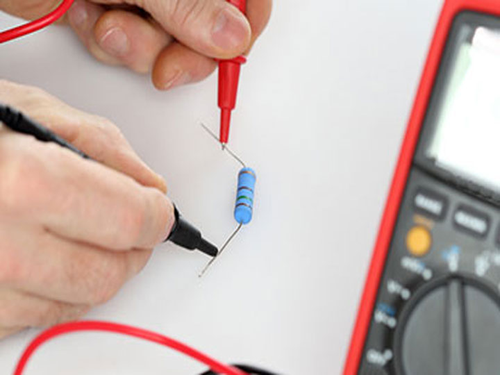
Just like any electronic product, PCBs need to undergo testing before they are shipped. Testing helps to confirm whether the printed circuit board is working correctly. Some methods for testing the board after PCB assembly design are as follows:
Quick visual inspection to ensure all electrical components are installed correctly.
Analog signature analysis: this involves using AC current in the two areas of the circuit and electrical components.
Functional testing: this helps to verify whether the printed circuit board is achieving its intended purpose.
Online testing: this involves checking many parameters, such as frequency and voltage.
Monitoring output helps to determine whether the PCB manufacturing process is progressing smoothly. One good way to achieve this is to investigate all detected faults. The optical inspection stage is the best time to do this, as it usually takes place after soldering. Therefore, all defects can be quickly identified and rectified before mass-producing printed circuit boards with the same issue. Today, printed circuit boards have many uses. From televisions to microwaves to anything in between, PCB is almost ubiquitous in the world of electronics.