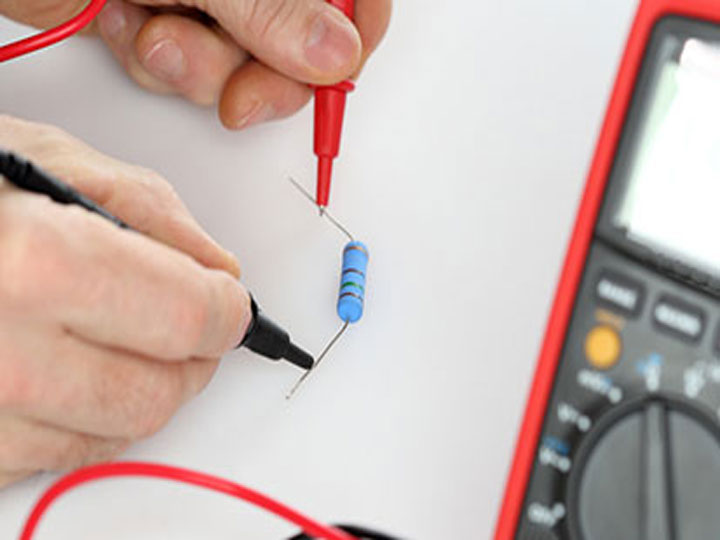

Basically, the purpose of setting inspection points is to check whether the components on the circuit board meet the specifications and characteristics. For example, if you want to check whether there is any problem with the resistance on a circuit board, the easiest way is to use a multimeter to measure it. You can find out by measuring both ends.
However, in a mass-produced factory, there is no way for you to use an electric meter to slowly measure whether the circuit of each resistor, capacitor, inductance, or even IC on each board of the printed circuit board is correct.
So there is the emergence of the so-called ICT automatic inspection machine, which uses multiple probes to contact all the parts lines on the board that need to be measured, and then sequentially measures these electronic components in a sequence-based and side-by-side manner through program control. Properties of the part.
Generally, it only takes about 1 to 2 minutes to complete the inspection of all parts of the printed circuit board in this way, depending on the number of parts on the circuit board. The more parts, the longer the time.
However, assuming that these probes directly contact the electronic components on the board or their solder feet, it is likely to crush some electronic components, but it will be counterproductive.
So a smart engineer made a clear "inspection point", and led out a pair of small circular dots at both ends of the part. There is no solder mask (mask) on it, so that the probes used for inspection can touch these small dots without using Direct access to those printed circuit board electronic components being measured.
In the early days of the circuit board, it was still a traditional plug-in (DIP) era, and the solder feet of the parts were indeed used as inspection points, because the solder feet of traditional parts were strong enough to not be afraid of needle sticks, but there were often probes. Misjudgment of poor contact occurs.
Because the general electronic parts are subjected to wave soldering or SMT tin, a residual film of solder paste flux is generally formed on the surface of the printed circuit board solder. The impedance of this film is very high and often constitutes the probe. The contact is poor, so the inspection operators on the production line are often seen blowing desperately with an air spray gun, or wiping the panels that need to be inspected with alcohol.
However, with the evolution of technology, the size of the circuit board is getting smaller and smaller. It is already a little laborious to squeeze so many electronic parts on the small circuit board. Therefore, the problem of the inspection point occupying the circuit board space is often planned. A tug of war between the end and the manufacturing end.
The appearance of the inspection point is generally round, because the probe is also round, which is easier to produce and relatively simple, so that the adjacent probes are close to each other, so that the needle density of the needle bed can be increased.
1. The use of needle bed for circuit inspection will have some inherent constraints on the mechanism. For example, the minimum diameter of the probe has a certain limit, and the needle with too small diameter is easily broken and damaged.
2. The distance between the needles is also bound to a certain extent, because each needle must come out from a circuit board hole, and a flat cable must be soldered to the rear end of each needle, assuming that the adjacent holes are too small, in addition to the problem of contact shorting between pins, and the intervention of the flat cable is also a big problem.
3. Needles cannot be planted around some high parts. Assuming that the probe is too close to the high parts, there is a risk of bumping the high parts and causing damage. In addition, because the parts are high, holes should be made on the needle bed seat of the inspection tool to avoid it, which directly means that the needle cannot be implanted. It's getting harder and harder to accommodate checkpoints for everything underground on a circuit board.
4. Because the board is getting smaller and smaller, the number of inspection points has been repeatedly commented on. Now there are some methods to reduce inspection points, and there are other inspection methods that want to replace the original needle bed inspection. None of the tests seem to be able to replace ICT 100%.