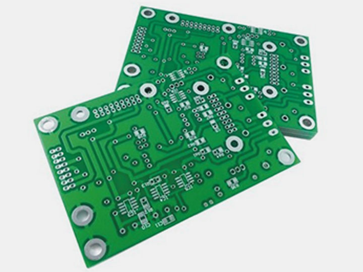
With the miniaturization of electronic products, there are about eight methods for assembling components on circuit boards during production, which can be divided into: manual visual inspection, digital microscope, SPI solder paste inspection machine, automatic optical inspection (AOI), SMT first-piece inspection instrument, inline inspection, functional test (FCT), and automatic X-ray inspection, etc. Now, let us briefly introduce the main PCBA test technologies.
SPI Solder Paste Inspection Machine for PCBA test
The SPI solder paste inspection machine utilizes optical principles to calculate the height of the solder paste printed on the PCB through triangulation measurement. Its function is to detect and analyze the quality of solder paste printing, discover SMT process defects in advance, allow users to monitor production problems in real-time, reduce defects caused by poor solder paste printing, provide strong quality control support to operators, and improve process performance.
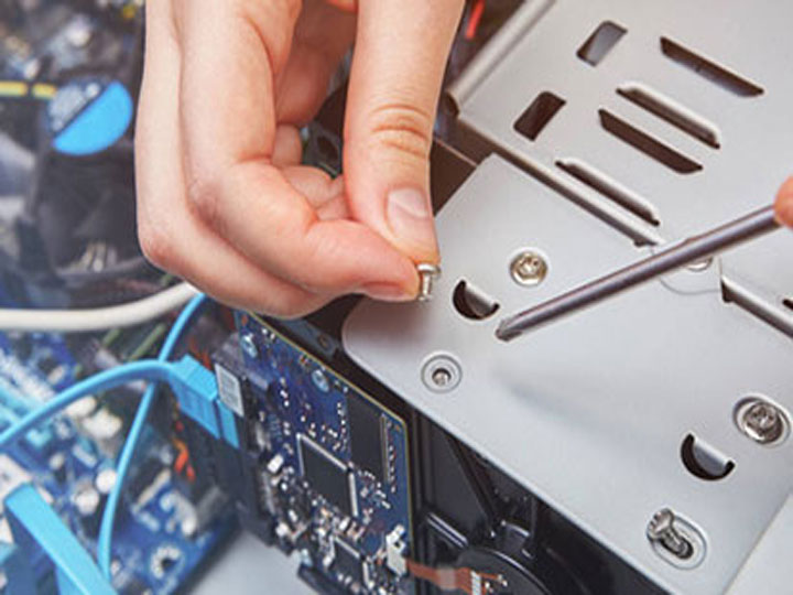
Manual Visual Inspection for PCBA test
Manual visual inspection for PCBA test refers to the use of human eyes with or without illumination of magnifying glasses to visually inspect the appearance, missing components, wrong components, polarity reversal, deviation and other quality issues of printed circuit boards and solder joints.
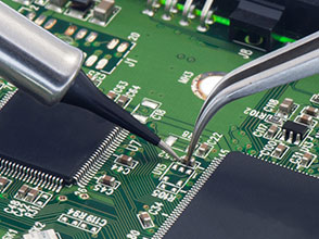
Digital Microscope for PCBA test
The digital microscope converts the image of the real object seen under the microscope into a digital signal. It magnifies the image of the real object and displays it on a computer screen. It can save and print images and measure various data using measurement software. Application: suitable for inspection of electronic industry production lines, inspection of printed circuit boards, inspection of soldering defects in printed circuit components, etc.
SMT First-piece Inspection Instrument for PCBA test
The SMT first-piece inspection instrument automatically inputs measurement data by integrating CAD coordinates, BOM tables, and the first PCB scanning image, simplifying the inspection of SMT production line products. The LCR reading data automatically corresponds to the corresponding position. The inspection results are judged from west to east to eliminate errors and omissions in test. The test report is automatically generated and stored in a database.
Automatic Optical Inspection for PCBA test
Automatic optical inspection (AOI) is a new type of technology that uses optical and digital imaging technology, as well as computer and software technology, to analyze images for automatic inspection. AOI automatically scans the printed circuit board through a camera, collects images, compares the tested solder joints with the qualified parameters in the database, detects defects on the PCB through image processing, such as missing components, wrong components, bad components, solder balls, offsets, tilted components, reverse installation, inverted pins, bridging, virtual soldering, no soldering, insufficient or excessive soldering, floating components, IC lead bending, and marks the defects on a display or automatically. This provides maintenance personnel with correction instructions.
X-ray Inspection for PCBA test
Automatic X-ray inspection is a new type of technology that uses X-rays to penetrate materials, discover defects in materials by attenuating characteristics, and mainly inspect internal defects of solder joints, such as BGA, CSP, and FC chip solder joint inspection. X-rays can penetrate the surface of an object and visualize the internal structure of the tested solder joints, which can be used to detect and analyze various common welding quality defects of electronic components. The X-ray inspection can fully reflect the welding quality of the solder joints, including open circuit, short circuit, holes, bubbles, tin content, etc., and can achieve quantitative analysis. The biggest feature of X-ray inspection is that it can detect solder joint defects under BGA encapsulated components, such as bridging, open circuits, missing solder balls, displacement, insufficient pin material of tested objects, voids, fuzzy edges of solder joints, and other internal defects.
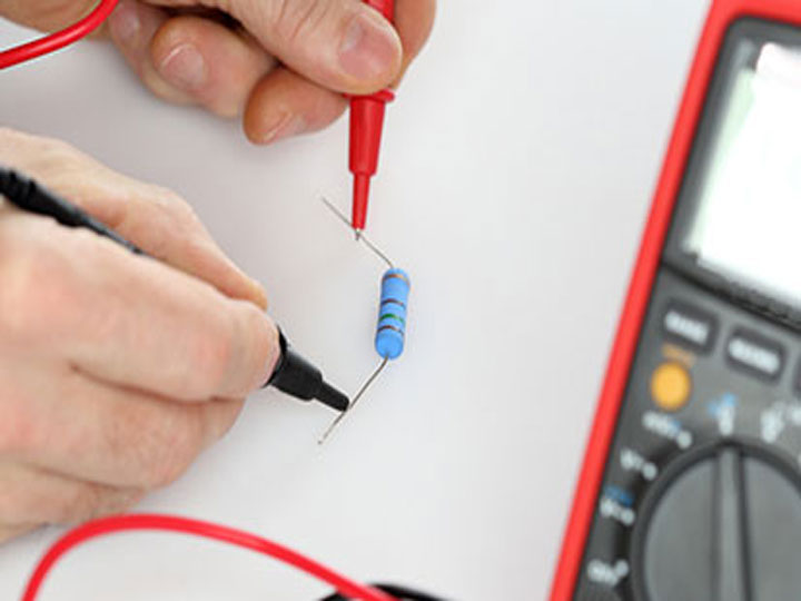
Inline Inspection for PCBA test
Inline test is a standard test method that checks for manufacturing defects and defective components by test the electrical performance and connection of online components. The dedicated pin bed contacts the solder joints of the components on the assembled circuit board, and discrete isolation tests are conducted with a voltage of several hundred millivolts and a current of less than 10mA to accurately measure component omissions, parameter value deviations, continuous soldering of solder joints, open or short circuits of the circuit boards, etc.
Functional test for PCBA test
Functional test for PCBA test provides an analog running environment to test the circuit board, allowing the circuit board to function under design conditions, obtain output, and verify the functional status of the circuit board. Simply put, the assembled electronic equipment's dedicated circuit board is connected to the appropriate circuit of the device, and then voltage is applied. If the device works properly, the circuit board is qualified.