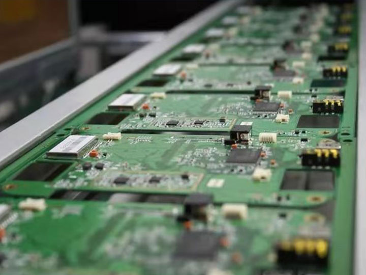
When it comes to PCB, we are all familiar with it, but do you know what PCBA is? PCBA refers to the assembly of PCB board through SMT patch, DIP plug-in, test and other processes to make it a finished product. We can understand it as a finished product circuit board. The PCBA test is to test the conductivity and input-output values of the PCBA board, why does PCBA need to be tested?
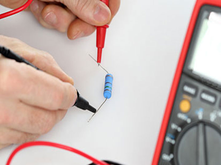
The production and processing technology of PCBA technology is very complicated, including the production of PCB boards, the procurement and test of electronic components, SMT patching, DIP plug-ins, and many other processes. In the production factory, various problems may be caused due to various reasons. Therefore, professional test equipment is needed, such as using a multimeter for test, to confirm the completeness of the design of the PCBA board.
Improve the production capacity of enterprises: the higher the pass rate of PCBA test, the higher the pass rate of products, which improves the product quality and promotes the production capacity of enterprises.
Enhance the economic benefits of enterprises: only products that have passed the test will be favored by users. In the test process, errors can be discovered and adjusted in time to make the product more perfect. Then the product can be put into the market and be favored by customers, which stimulates the development of the economic benefits of enterprises.
ICT test: test circuits, currents, voltages, amplitudes, and noise.
FCT test: test the functions of PCBA, such as whether the LED light can be turned on after pressing the button, and whether it can restore the factory settings.
Fatigue test: sample high-frequency and long-term operations to observe whether the faults will occur, and determine the probability of failures, so as to understand the performance of PCBA technology board.
Extreme environment test: place the PCBA board in harsh extreme environments, such as high temperature, low temperature, and dropping, and calculate the reliability of the PCBA board based on the test results.
PCBA test is an indispensable important link to ensure the quality of product delivery, which determines the performance of the product, controls the quality of the product, reduces the after-sales and repair rate, makes customers more confident, and promotes the win-win cooperation between enterprises and customers.
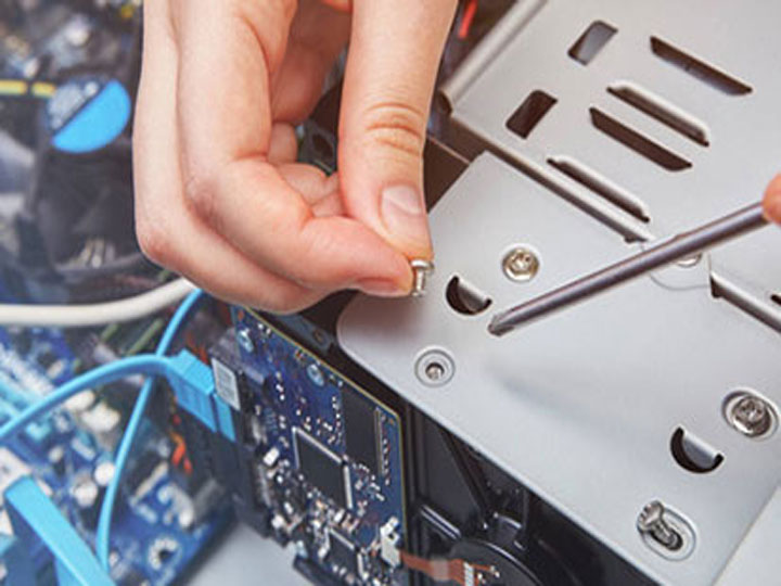
The basis for PCBA processing rework and repair
PCBA processing rework and repair should be carried out according to the PCB design files and repair regulations, and there should be a unified process specification for rework and repair.
The number of rework times allowed for each solder joint
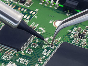
Rework is allowed for defective solder joints, and the number of rework times for each solder joint should not exceed three times, otherwise it will cause damage to the soldering part.
The use of removed components
Removed components should not be used again. If necessary, they must be screened and tested according to the original electrical and process performances of the components before they can be installed.
The number of desoldering operations allowed on each solder pad
Each printed solder pad should only undergo one desoldering operation (that is, only one component replacement is allowed). The thickness of the metal intermetallic compound of a qualified solder joint is 1.5-3.5 µm. After remelting, the thickness will increase, and even reach 50 µm. The solder joint becomes brittle, and the welding strength decreases, which poses serious reliability risks under vibration conditions. Moreover, remelting IMC requires a higher temperature, otherwise IMC cannot be removed. The copper layer at the through-hole exit is the thinnest, and the solder pad is easily broken from this position after remelting; the copper layer undergoes deformation due to the thermal expansion of the Z-axis. Due to the obstruction of the lead-tin solder joint, the solder pad may detach.
In the case of lead-free, the entire solder pad will be pulled up, and the PCB will be layered due to the moisture between the glass fiber and the epoxy resin. After heating, the solder pad is prone to warping and separation from the substrate due to multiple welding.