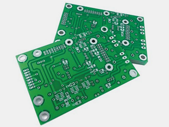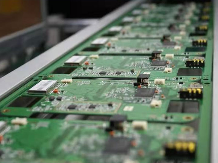
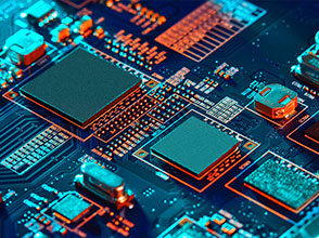
PCB is short for printed circuit board, which is an important electronic component that provides electrical connections for electronic components and supports them. As it is produced using electronic printing technology, it is known as a "printed" circuit board. PCB fabrication services can be divided into single-sided boards, double-sided boards, four-layer boards, six-layer boards, and other multilayer boards according to the number of layers.
Firstly, the schematic diagram is designed according to the project requirements using circuit design software. The PCB layout is drawn based on the schematic diagram. Secondly, the board is cut to the required size based on the size of the circuit board. Then, holes are drilled for screws and fixed mounting holes. Finally, after processes such as copper sinking, electroplating, film removal, etching, green oil, silk screen characters, molding, and testing, a PCB fabrication board can be produced.
The relationship between line width, hole size, and the current passing through the PCB
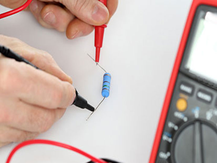
The copper foil thickness of a general PCB fabrication board is 1 ounce or about 1.4 mil, and the maximum current allowed for a 1 mil line width is 1A. The size of the hole is more complicated and not only related to the size of the hole pad but also to the thickness of the copper deposited on the hole wall during processing.
Convert PCB files to GERBER files and drill data before submitting them to the PCB factory
Because electronic engineers and PCB engineers have different understandings of PCB design, the GERBER files converted by the PCB factory may not be what you want. For example, if you define the parameters of the components in the PCB file during design and do not want these parameters to be displayed in the finished PCB, but do not specify this instruction, the PCB factory will keep these parameters on the finished PCB. Therefore, converting PCB files to GERBER files is more accurate for PCB fabrication.
Improve the via rate
To complete the design of a printed board diagram, the process usually goes through schematic input-network tabulation-definition-network table (component) loading-component layout-automatic (manual) wiring, etc. Functions can automatically move components to grid intersections, which is very beneficial for increasing the via rate.
After automatic copper coverage, the copper coverage will fill the blank spaces according to the position of the components and the layout of the traces on the board
However, this will form many acute angles and burrs less than or equal to 90 degrees, which will discharge during high-voltage testing and cannot pass the high-voltage test. There is no other good way except manually correcting these sharp corners and burrs stage by stage after automatic copper coverage.