
The main innovation in electronic fabrication is the printed circuit board. This makes updating PCB layout and assembly a crucial challenge for electronic manufacturers and OEMs. During PCB assembly, solder bridges pose a daunting challenge for both PCB fabrication manufacturers and customers. This article is a brief guide for all original equipment manufacturers to understand the importance of solder masks during PCB assembly and PCB layout to prevent solder bridges. It will also help you understand the root causes and prevention measures to avoid solder bridges during the PCB assembly process, and prevent damage to components and circuit boards, leading to PCB rework.
For creating perfect PCB prototypes, PCB layout and assembly stages play a crucial role in deducing suitable electronic fabrication and design solutions. Whether it is for PCBs used in aerospace, defense, military, renewable energy, transportation, telecommunication, or any other industry, PCB fabrication manufacturers need to use high-quality raw materials to develop meticulously crafted PCB fabrication processes and provide accurate PCB layouts to prevent solder bridges or PCB rework, providing highly durable and effective solutions to save time and money for electronic manufacturers.
To understand what to consider during PCB assembly, all electronic manufacturers should first understand the common major issues to be considered. Among them, solder bridges are a major concern. Understanding the importance of solder bridges is therefore crucial.
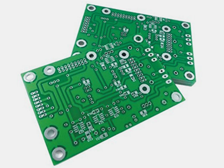
Solder bridges are unwanted accidental electrical connections between conductors due to a small piece of solder. They are also referred to as "short circuits" in PCB terminology. Detecting solder bridges can be difficult when dealing with fine pitch components. If not resolved, it can lead to damage to other components and circuit boards. A solder mask (that is, a thin layer of polymer applied to the copper traces on the printed circuit board) is applied to protect them from oxidation and to prevent the formation of solder bridges between pads. This solder mask is essential for mass production of PCBs, but its use is less frequent for hand-soldered PCB components. For circuit boards that require automated soldering, the trend for solder baths and reflow soldering is high. To avoid solder bridges during PCB assembly, first determine the appropriate type of solder mask used during PCB assembly. This will become a sensitive consideration factor when acquiring proper PCB layout and PCB types for your project.
Electronic manufacturers should thoroughly investigate the pros and cons of each type of solder resist film and then decide whether to opt for epoxy liquid, liquid photoimageable solder resist, or dry film photoimageable solder resist. They can even help PCB fabrication manufacturers with consultations and seek a perfect PCB assembly process through clearly defined technologies and PCB production processes. For all electronic product manufacturers, while preventing solder bridges may entail extra time and money investment, it can help you achieve significant long-term returns.
The primary cause of solder bridges is improper PCB layout. The demand for introducing more compact and faster technology has increased as well as the idea of combining packaging size and material use inadequately. This is a significant challenge for OEMs and requires a perfect and appropriate PCB layout. They often end up compromising on PCB fabrication layouts to launch new products in the market. Other causes of solder bridges include a lack of solder resistive between solder pads on the circuit board. Insufficient polymer layer, called solder mask, on copper traces of the PCB also leads to solder bridge problems. Improper spacing ratios of solder pads become a cause of solder bridges when the device pitch is 0.5mm or less. Improper template specifications lead to excessive solder paste, leading to solder bridges. These are common problems that cause solder bridges during PCB assembly due to improper sealing between the PCB and solder paste template, incorrect template thickness, errors during surface-mounted component placement or poor distribution of solder paste compared to the PCB.
Validate whether each wire is coated with a solder resist and if it is not used strictly due to tolerance, it explains the design changes around that particular component. Recommended solder mask templates with 0.127mm thickness, with stainless steel templates cut by laser, are also suitable for 0.5mm device pitch. These are preventive measures to avoid solder bridges and get the perfect PCB assembly solution.