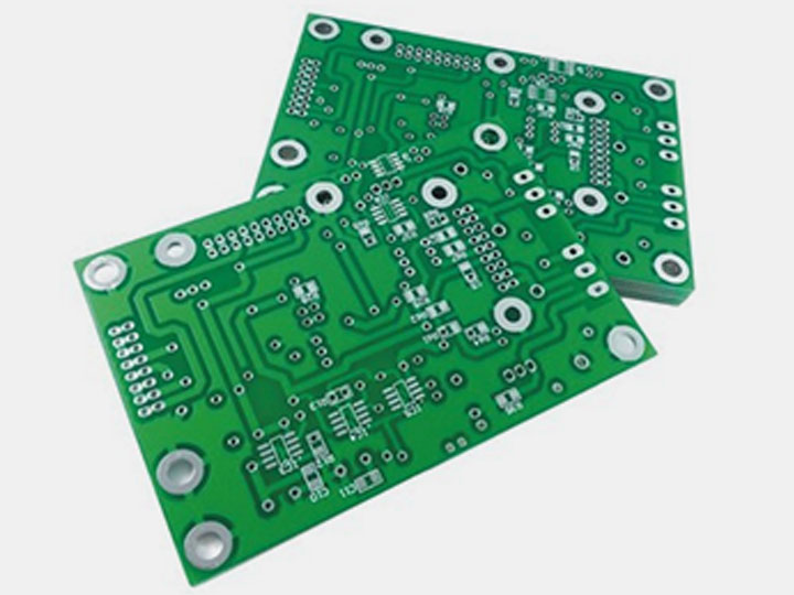

PCB board must be selected to meet the design requirements and mass production and cost to achieve a balance. Design requirements include both electrical and mechanical parts. Usually in the design of a very high-speed PCB board (greater than GHz frequency) when the material issue will be more important. For example, now commonly used FR-4 material, in a few GHz frequency dielectric loss will have a significant impact on signal attenuation, may not be suitable. In terms of electrical, we should pay attention to the dielectric constant, and dielectric loss in the designed frequency is suitable.
The basic idea of avoiding high-frequency interference is to minimize the interference of the high-frequency signal electromagnetic field,
which is also called crosstalk. The distance between the high-speed signal and the analog signal can be enlarged, or add ground guard/shunt traces in the analog signal next to. Also, pay attention to the digital ground to the analog ground noise interference.
Signal integrity is basically a matter of impedance matching. The factors that affect impedance matching are the architecture of the signal source and output impedance, the characteristic impedance of the alignment, the characteristics of the load side, the topology of the alignment architecture, etc. The way to solve the problem is to rely on termination and adjust the topology of the line.
Each PCB assembly frame is connected to each other between the signal or power in the action. For example, a board has power or signal to the
B board, there must be an equal amount of current flow from the ground back to the Aboard. The current on this ground level will find the place with the lowest impedance to flow back. Therefore, the number of pins assigned to the ground layer cannot be too small at each interface regardless of power or signal interconnection to reduce the impedance, which can reduce the noise on the ground layer. In addition, you can also analyze the entire current loop, especially the part of the current is larger, adjust the ground layer or ground connection to control the way the current goes (for example, to create a low impedance at a certain place, so that most of the current goes from this place), to reduce the impact on other more sensitive signals.
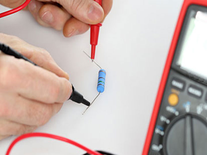
In the design of a high-speed PCB circuit, impedance matching is one of the elements of the design custom PCB. The impedance value and the way
the alignment has an absolute relationship, for example, is to go in the surface layer (microstrip) or the inner layer (stripline/double stripline), and the reference layer (power layer or ground layer) distance, the width of the alignment, PCB material, etc. will affect the characteristic impedance value of the alignment. In other words, the impedance value can be determined only after the wiring. General simulation software will be due to the line model or the limitations of the mathematical algorithm used and can not take into account some impedance discontinuity in the wiring situation, which can only be reserved in the schematic diagram some terminators (termination), such as series resistors, etc., to moderate the effect of discontinuity in the impedance of the line. The real fundamental solution to the problem is to avoid the occurrence of impedance discontinuity when wiring as much as possible.