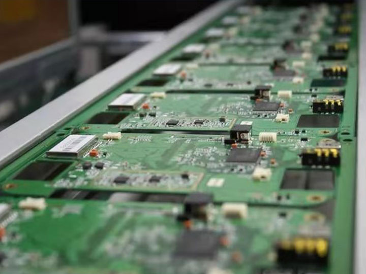
The development of the technology for BMS PCBs (PCBs) is accompanied by advances in material technology. According to the hardness of the insulation layer material, PCBs can be divided into rigid, flexible, and rigid-flex PCBs. Taking rigid-flex PCBs as an example, compared with traditional rigid-flex PCBs, the newly developed technology allows flexible PCBs to be integrated into rigid PCBs. This greatly reduces the weight of electronic devices and avoids the drawbacks of complex, bulky, and difficult-to-repair production processes. At the same time, the flexible area of the new PCB can be bent repeatedly and twisted at any angle, which increases its scope of application to a certain extent.
Flexible substrates, such as polyimide, have high dielectric stability. When applied in PCBs, they can provide good dielectric properties and electrical performance, and in high-speed and high-frequency signal transmission as well as impedance control, they can play to their strengths. Additionally, rigid-flex PCBs also demonstrate stability under harsh and extreme conditions, such as lightning, high-frequency heating, pulse corrosion, and spark machining, and exhibit some resistance.
The anti-interference design for BMS PCB is closely related to the specific circuit. The design of the circuit should take into account the overall information of the PCB, the density of the signal lines, and power factors, etc. In order to prevent interference, a high stability, low output impedance DC power supply should be used. Also, on the basis of ensuring the required power supply and wiring layers of the circuit function, the ground connection of the output should be as close as possible to the earth of the power supply. In electronic circuits, the grounding wire requires a thick main line to reduce the circuit loop resistance.
Secondly, the width of the power supply line should be increased as much as possible, and the principle should be that the interference spike on the power supply line will not cause the output state of the logic device to change, eliminating the interference caused by the suppression of the DC power supply circuit due to changes in the load. In the face of power supply interference, a shield layer can be installed between the primary winding and the secondary winding of the power supply transformer or a power supply filter can be added to reduce the interference caused by electromagnetic waves. In addition, between the signal sending line and the receiving line, or between the same signal lines, the parallel walking line should be avoided as much as possible. If the signal lines are not compatible, isolation treatment should be carried out to prevent the formation of coupling interference.
The decoupling capacitor between the power and ground of integrated circuitry has two functions: one is the energy storage capacitor of the integrated circuit, and the other is to bypass the high-frequency noise of the device. In order to weaken the interference signal coupling path, the signal line should be as short as possible, unnecessary stray capacitance should be minimized, and the signal line routing should be arranged in a certain order. The clock signal and sensitive signal lines should come first, followed by high-speed signal lines, and finally non-critical signal lines.
In order to prevent coupling interference between signal lines, the system should reduce false operations and minimize outward radiation. In addition, since transient currents are much larger than static currents, power supply decoupling measures can be taken to reduce interference and current consumption. Two capacitors are connected between the power supply line and the ground line to play the roles of energy storage and noise bypass for the integrated circuit. In this process, attention should be paid to the fact that the capacitor leads should not be too long, especially for high-frequency bypass capacitors. The pins of the decoupling capacitor should be as short as possible during soldering to avoid self-resonance of the capacitor caused by excessively long leads. Finally, to minimize noise coupling and crosstalk between adjacent lines on the same layer, isolation treatment should be carried out between the lines.