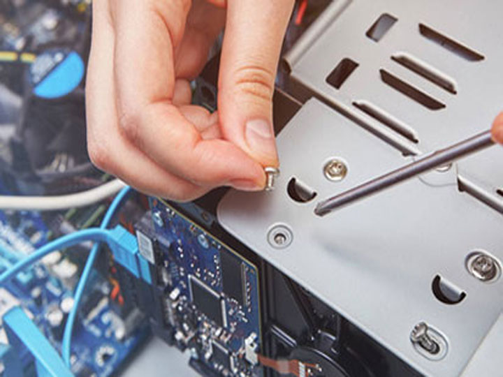
BMS PCB can be classified into flexible boards, rigid boards and rigid-flex boards according to their structure, and into single-sided boards, double-sided boards and multi-layer boards according to the number of layers. They can also be used for different purposes such as civil and military use, each requiring different production processes and technologies. Currently, high-density interconnect BMS PCBs have a dominant market position due to high demand. These circuit boards have more precise lines and require high interlayer positioning accuracy. Compared to traditional circuit boards, they have better electrical performance and signal integrity, and are suitable for increasingly complex electronic packaging processes. For such BMS PCB, interconnection hole processing, hole metallization processing, and precision line production technologies are mainly employed. For high-density interconnect BMS PCB, mechanical drilling and laser drilling methods can be used for blind hole and through-hole processing. Different methods and processing parameters should be adopted for different substrate materials.
After drilling, the hole walls of the BMS PCB need to be metallized to achieve interlayer connection. Currently, the commonly used methods are chemical copper plating and carbon black hole methods, both of which require subsequent electroplating processes to metallize the hole walls. The uniformity of the current distribution of electroplating has a significant influence on the copper plating ability. The production of precision lines is an important direction for the development of BMS PCB. Currently, the most mature production method is the subtractive method, and the precision of this technology will have a decisive effect on the performance of BMS PCB in the future.
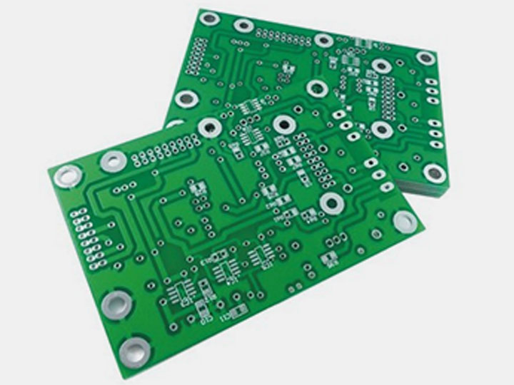
The substrate is the core part of the BMS PCB carrying the functional circuit, and the substrate's characteristics determine the circuit board's environmental adaptability. Currently, the most widely used substrate is an epoxy glass cloth substrate, which has high strength, chemical and moisture resistance, excellent thermal stability, good electrical properties, and provides good protection for BMS PCB. For line production, to reduce process time and cost while ensuring quality, a method can be adopted to produce lines on ultra-thin copper foils by controlling the electroplating time to adjust the line's thickness and produce precision lines. In the exposure process, light-sensitive oligomers in the dry film will undergo a polymerization reaction and protect the circuit in subsequent processes. Therefore, the exposure process is a key step in making precision lines. Non-parallel exposure machines and direct laser imaging exposure machines are currently the most advanced exposure technologies, and they can avoid the impact of environmental factors such as temperature and humidity on line production, and have great advantages in making fine lines with fixed line widths or line intervals.
In the production process of BMS PCB, defects are inevitable, and the purpose of anti-interference performance testing is to indirectly identify the location information of defects through an analysis of the performance of BMS PCB and take timely measures. At present, the main methods for determining the performance of BMS PCB products mainly focus on short circuits, open circuits, pinholes, gaps, and line oxidation. In the defect detection of BMS PCB, reference-based defect detection is mostly used, and the main idea is to compare the measured image with the standard image. For example, using a fully automatic exposure machine to take photos, the position difference of the image is extracted and calculated to determine the deviation level of the BMS PCB.
Different defects have different characteristics in the obtained images. For example, if there are many pixel clusters in one position, it is a short circuit. If there are partially bright areas on a black background, it indicates that the area may be a defect such as burrs or pinholes, etc. Line oxidation is a defect that severely affects the conductivity of the line due to improper external control during the production process. As a non-fatal defect, line oxidation can be distinguished by the difference in copper wire color, making it simple and practical in the anti-interference performance testing of BMS PCB.