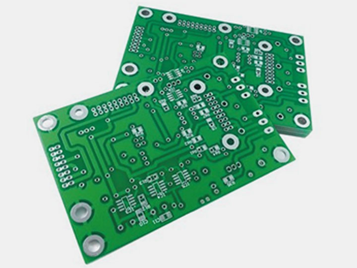

In the production process of PCBA SMT, defects in PCBA technology placement such as soldering, short circuit, warping, missing components, solder beads, bent pins, high floating, wrong placement, cold welding, reverse placement, reverse side, offset, component damage, less solder, more solder, gold finger soldering, glue overflow, etc. can easily occur due to operation errors. These defects need to be analyzed and improved to improve product quality.
Weak specificity of red glue; poor opening of the mesh plate; the distance between the copper foil is too large or the large copper paste small components; the pressure of the scraper is too high; poor component flatness (bent pins, deformation); too fast temperature rise in the preheating zone of the reflow oven; the copper foil in the PCB is too dirty or oxidized; the PCB board contains moisture; SMT machine placement shift; offset in red glue printing; machine clamp track loosening causes component placement shift; misalignment points lead to component offset, resulting in soldering voids.
Too large distance between the mesh plate and the PCB design board results in over-thick red glue and short circuit; the component placement height is set too low, which will squeeze the red glue and cause short circuit; too fast temperature rise in the reflow oven; component placement offset; poor mesh opening (thickness is too thick, pin openings are too long, holes are too large); the red glue cannot bear the weight of the component; deformation of mesh or scraper causes over-thick red glue printing; red glue has strong specificity; the glue paper of the empty sticking point is rolled up, causing over-thick red glue printing around the components; large or non-horizontal vibration during reflow soldering.
Uneven tension caused by different sizes of copper pads on both sides; too fast temperature rise and no uniform thickness of red glue printing; component placement offset; uneven distribution of temperature in the reflow oven; offset of the red glue printing; machine track clamp loosening causes placement offset; machine head shaking; red glue specificity is too strong; improper furnace temperature setting; too large distance between copper pads; component placement offset caused by misalignment points.
Faulty carbon film of the vacuum pump or insufficient vacuum lead to missing components; clogged suction nozzle or faulty suction nozzle; improper component thickness test or defective detector; improper component placement height; excessive or no air blowing of the suction nozzle; improper vacuum setting of the suction nozzle (applicable to MPA); too fast placement speed of special-shaped components; broken head air pipe; wear of the air valve sealing ring; foreign objects on the rail of the reflow oven wiping off the components on the plate.
Insufficient preheating of the reflow soldering, too fast temperature rise; incomplete reheating of the red glue after refrigeration; splashing caused by moisture absorption of the red glue (indoor humidity is too high); too much moisture in the PCB design board; excessive addition of diluent; poor design of mesh plate opening; uneven tin powder particles.
The positioning reference point on the circuit board is not clear; the positioning reference point on the circuit board is not aligned with the reference point on the mesh plate; the fixing fixture of the circuit board in the printer is loose, and the top needle of the positioning mold is not in place; the optical positioning system of the printer is faulty; the solder paste leakage does not meet the design file requirements of the mesh plate opening and the circuit board. To improve the defects in PCBA technology placement, strict inspections need to be carried out at each stage to prevent problems from flowing from the previous process to the next as much as possible.